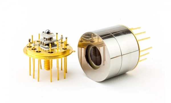
PVA/PVIA InAs/InAsSb Photovoltaic Detectors


Top seller


 Photovoltaic Detectors Vigo System")
 Photoconductive Detectors Vigo System")

 Infrared Detector Arrays Vigo System")


Viewed